

Samsung has launched its SAFE (Samsung Advanced Foundry Ecosystem) Cloud Design Platform (CDP), designed in collaboration with Rescale for the company’s fabless customers. The platform provides a virtual environment where Samsung Foundry’s customers can develop chips in the cloud.

The key highlight feature of Samsung foundry’s first SAFE™ Cloud Design Platform is that it provides a virtual environment to design chips in the cloud. By accessing this platform through the cloud, customers can immediately start designing at anytime and anywhere.
To maximize customers’ design convenience, SAFE™ CDP supports a very secure design condition that has verified with cloud companies. In addition, customers can utilize various Electronic Design Automation (EDA) tools offered by multiple vendors such as Ansys, Cadence, Mentor, a Siemens business and Synopsys.
Gaonchips, one of Samsung Foundry’s Design Solution Partners, has already tested the SAFE™ CDP on its 14nm automotive project using Cadence’s Innovus Implementation System and has successfully reduced its design run-time by 30 percent compared to current on-premise execution.
“We expect that our innovative design platform co-developed in partnership with Rescale will play a crucial role for the fabless industry as it evolves into efficient cloud-based design environment,” said Jae-hong Park, executive vice president of Foundry Design Platform Development at Samsung Electronics.
“We remain committed to our efforts to bolster the SAFE™ ecosystem and will continue to collaborate with our SAFE™ partners on developing innovative programs that will help deliver ease of use and greater design efficiency for customers.”
Samsung Foundry first launched SAFE in 2018, lowering the barrier for its customers to develop competitive SoC (System on Chip) designs. SAFE CDP is an extension to that, and it allows fabless customers to design chips anytime and anywhere.
As designs move to advanced nodes and as transistor scaling occurs at each node, chip designs become more complex and computing power required for these designs have increased significantly, resulting in greater overhead time and cost to customers.
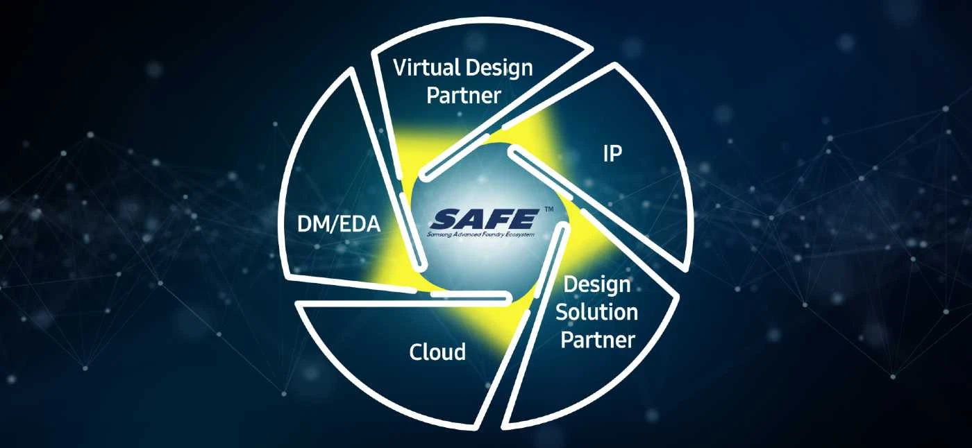
By adopting CDP, customers can reduce the burden of building their own server infrastructure, while flexibly utilizing additional computing power required for chip design and verification. Furthermore, they can take full advantage of Samsung’s diverse foundry ecosystem which includes EDA, intellectual property (IP), cloud, and design services offered by reputable partners.
“We are excited to be a partner of Samsung Foundry SAFE™ ecosystem,” said Joris Poort, founder and CEO of Rescale. “We share a common vision of a global design cloud platform that efficiently supports a broad ecosystem of technologies and services for EDA customers worldwide.”