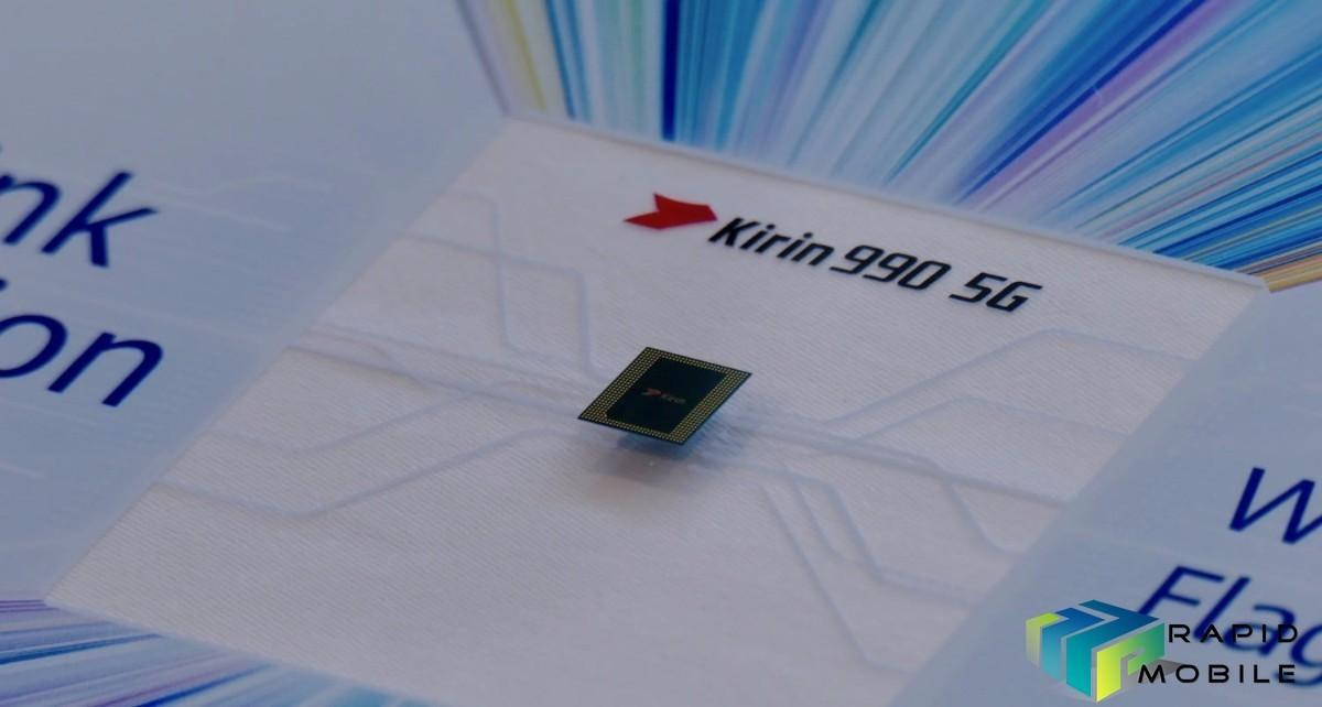
Huawei unveiled the Kirin 990 and Kirin 990 5G chipsets. Surprisingly, 5G compatibility won’t be included automatically in every Kirin 990-equipped smartphone. Instead, there will be two versions of the chipset, one with 5G and one without.
The two Kirin chipsets have same core configuration, same camera support, same memory, same storage. However, in a few key areas beyond the modem, there are differences, such as NPU performance and core frequencies.
The Kirin 990 will power Huawei’s forthcoming flagship smartphone, the Mate 30, which is due for release on September 19.
The new chip is an eight-core part, with those cores split into three groups: two ‘big’ full-power Cortex-A76 based cores running at 2.86GHz for dealing with demanding tasks; a pair of mid-power cores – also Cortex-A76 based – running at 2.36GHz; and four Cortex-A55 based cores running at 1.95GHz.
Graphics are dealt with by a 16-core Mali-G76 GPU and the chipset is built on a hybrid 7nm FinFet and EUV (extreme ultraviolet lithography) manufacturing process.
the 5G chip should be integrated on the same silicon, enabling better efficiency in 5G mode in exchange for die area and design complexity.
Huawei are the first company to integrate the 5G chip on the same silicon, enabling better efficiency in 5G mode. The Kirin 990 5G is a true unified design, supporting Sub-6 GHz 5G networks on both SA and NSA architectures. In order to keep the die size in check, Huawei is using TSMC’s latest 7+ manufacturing process with EUV, which helps enable a smaller die size for the sorts of devices this chip will be going into.
One of the key elements to the Kirin 990 5G is its use of TSMC’s 7FF+ with EUV, which enables the chip to have a small(er) die size. The chip is over 100mm2, which is up from 74.13 mm2 on the Kirin 980 (TSMC 7nm) and 96.72 mm2 on the Kirin 970 (TSMC 10nm), possibly making it Huawei’s largest smartphone SoC to date.
This is compared to the Kirin 990 4G version, which is around ~90 mm2, but is built on the same 7nm process as the Kirin 980, making it a little bigger. Transistor counts for the two chips put the 990 5G at 10.3 billion, while the 990 4G is ~8 billion.
The core configuration on both SoCs is the same – two high frequency A76 cores, two medium frequency A76 cores, and four more efficient A55 cores. These are split into their own power and frequency domains, allowing better flexibility based on workload. However, the 990 5G and 990 4G will both have slightly different frequencies, based on the differences between the 7 and 7+ processes.
| Huawei Kirin Family | ||||
| AnandTech | Kirin 990 5G |
Kirin 990 (4G) |
Kirin 980 | Kirin 970 |
| CPU | 2xA76 @2.86G 2xA76 @2.36G 4xA55 @1.95G |
2xA76 @2.86G 2xA76 @2.09G 4xA55 @1.86G |
4xA76 @2.60G 4xA55 @1.80G |
4xA73 @2.36G 4xA53 @1.80G |
| GPU | G76MP16 @700M |
G76MP16 @700M |
G76MP10 @750M |
G72MP12 @850M |
| NPU | 2 + 1 Da Vinci |
1 + 1 Da Vinci |
2 Cambricon |
1 Cambricon |
| Modem | Balong 5G | 4G | 4G | 4G |
| DRAM | LPDDR4-4266
+ LLC |
LPDDR4-4266
+ LLC |
LPDDR4X-4266 | LPDDR4X-3733 |
| Die Size | >100 mm2 | ~90 mm2 | 74.13 mm2 | 96.72 mm2 |
| Transistors | 10.3b | ~8.0b | 6.9b | 5.5b |
For caches, the all four A76 cores have 512 kB L2, while the A55 cores are 128 kB each.
Technically Huawei calls the A76 cores as ‘A76-based’, because certain enhancements have been made to the core in the cache system to improve memory latency. Huawei wouldn’t dictate anything more than saying that its ‘SmartCache’ implementation, that helps the GPU, also helps the CPU and NPU as well.
For the graphics, the Kirin 990 parts will both have a 16-core Mali-G76 implementation, up from a 10-core Mali-G76 in the Kirin 980. This is partly for the reason for the increased die size: Huawei believes that a lower voltage, lower frequency but wider GPU will offer a better chip overall.


